
Laser Marking Electronics Industry Components
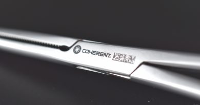
Laser Marking in the Electrical Goods and Electronics Industry Terminal strip.
No other market is as complex as the Electronics industry. There is much more to it than the chip production in Asia. A wide range of products manufactured in Europe and America also belong to this sector, e.g. plugs/ connectors, housings, sensors, transistors, switches resistors, capacitors and many more. While especially chip manufacturers produce in Asia, the European and American markets are characterized by small and medium sized enterprises specializing in the manufacture of components or plant and equipment machinery.

Challenges
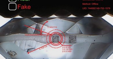
All electric and electronic products, components and parts have to be marked, identified or coded one way or another. The marking contents range from simple alphanumeric codes to complex 2D codes, logos or individual data. Often, the data that has to be appIied is very tiny as many substrates are extremely small. The range of substrates that have to be marked is wide and integration into machines, lines and clean rooms is an issue, too. Ergo: Laser markers have to be flexible and compact to be suitable for the electronics industries.
Solution
Laser marking is highly cost-effective for the electronics industries and offers the best quality with easily traceable marks. Alltec develops the latest and most effective systems suitable for the electrical goods, electronics and semiconductor industries.
Smallest and Finest Codes in the Shortest of Time
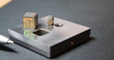
FOBA Laser Marking + Engraving proprietary scan technology which is incorporated in all systems delivers optimum marking quality at highest marking speeds. Our continuous wave fiber laser markers have been primarily designed to mark molded housings of discrete and integrated components as well as circuit boards, precisely, with high quality and in the shortest of time. With these systems line widths well below 30 μm can be achieved, enabling character heights of 150 μm and less. Materials The materials that are processed most commonly range from various plastics to ceramics, metals and various alloys. All these substrates can be laser marked. Depending on the respective material FOBA Laser Marking + Engraving can offer the optimal laser marker.
Integration
Due to their generally small sizes, their compact mechanical design and flexibility and the many available options (e.g. with/ without beam turn) our systems can be perfectly integrated into new and existing production lines and industrial electronic handling/ automation systems (e.g. assembly, packaging or handling machines). The smallest of them are the most cost-effective solutions for clean room environments.
(Photos provided by FOBA Laser Marking + Engraving)
For more Information: www.fobalaser.com